Overview
| Information | 2.25V to 3.6V Quad UART with 16-Byte FIFO |
|---|---|
| Data Bus Interface | Intel, Motorola |
| # of Channels | 4 |
| Max Data Rate 5V (Mbps) | na |
| Max Data Rate 3.3V (Mbps) | 4 |
| Max Data Rate 2.5V (Mbps) | 3.125 |
| Max Data Rate 1.8V (Mbps) | na |
| Tx FIFO (Bytes) | 16 |
| Rx FIFO (Bytes) | 16 |
| Auto Flow Control | |
| Auto RS-485 Half-Duplex Control | |
| Multidrop (9-bit) Mode | |
| Fractional Baud Rate Generator | |
| Power Down Mode | |
| Supply Voltage Range VCC (V) | 2.25 to 3.63 |
| Auto RTS/CTS | |
| Package | LQFP-64 |
| FIFO Level Counters | |
| Selectable/ Programable Trigger Levels | S |
| IrDA Sup | |
| 5V Tolerant Inputs | ✔ |
| Max UART/GPIO Input Voltage (V) | 5.5 |
| Max UART/GPIO Output Voltage (V) | VCC |
| Temperature Range (°C) | -40 to 85 |
The XR16V5541 (V554) is a quad Universal Asynchronous Receiver and Transmitter (UART) with 16 bytes of transmit and receive FIFOs, selectable receive FIFO trigger levels and data rates of up to 4 Mbps at 3.3 V. Each UART has a set of registers that provide the user with operating status and control, receiver error indications, and modem serial interface controls. An internal loopback capability allows onboard diagnostics. The V554 is available in a 48-pin QFN, 64-pin LQFP, 68-pin PLCC and 80-pin LQFP packages. The 64-pin and 80-pin packages only offer the 16 mode interface, but the 48- and 68-pin packages offer an additional 68 mode interface which allows easy integration with Motorola processors. The XR16V554IV (64-pin) offers three state interrupt output while the XR16V554DIV provides continuous interrupt output. The XR16V554 is compatible with the industry standard ST16C554.
NOTE: 1Covered by U.S. Patent #5,649,122
- Pin-to-pin compatible with ST16C454, ST16C554, TI’s TL16C554A and Philips' SC16C554B
- Intel or Motorola Data Bus Interface select
- Four independent UART channels
- Register Set Compatible to 16C550
- Data rates of up to 4 Mbps at 3.3 V and 3.125 Mbps at 2.5 V
- 16 byte Transmit FIFO
- 16 byte Receive FIFO with error tags
- 4 Selectable RX FIFO Trigger Levels
- Full modem interface
- 2.25V to 3.6V supply operation
- Crystal oscillator or external clock input
- Pb-Free, RoHS Compliant Versions Offered
- Portable Appliances
- Telecommunication Network Routers
- Ethernet Network Routers
- Cellular Data Devices
- Factory Automation and Process Controls
Documentation & Design Tools
| Type | Title | Version | Date | File Size |
|---|---|---|---|---|
| Data Sheets | XR16V554/554D 2.25V to 3.6V Quad UART with 16-Byte FIFO | 1.0.3 | July 2010 | 923.5 KB |
| Application Notes | DAN-189, MaxLinear UARTs in GPS Applications | 1.0.0 | April 2008 | 139 KB |
| User Guides & Manuals | XR16M654_ Evaluation Board User's Manual | 1 | April 2009 | 114.9 KB |
| Product Flyers | 2.25V tO 3.6V Quad UART with 16/32/64-Byte FIFO | 1.0.0 | December 2006 | 321.4 KB |
| Product Brochures | Interface Brochure | November 2023 | 3.7 MB | |
| Schematics & Design Files | PCI Eval Board Schematic | 1.1.0 | April 2009 | 212.8 KB |
| Schematics & Design Files | ISA Eval Board Schematic | 1.1.0 | September 2007 | 187.4 KB |
| Software: Drivers | Linux 2.6.13 | 1.0.0 | December 2009 | 10.8 KB |
| Software: Drivers | Linux 2.6.18 | 1.0.0 | December 2009 | 12.1 KB |
| Software: Drivers | Windows XP & 2000 | 1.3.0.0 | December 2009 | 61 KB |
Simulation Models
| Package Type | Vcc | Temp | Mode | Version | File |
|---|---|---|---|---|---|
| PLCC | 2.5V | Industrial | Intel | 1 | |
| PLCC | 2.5V | Industrial | Motorola | 2 | |
| PLCC | 3.3V | Industrial | Intel | 1 | |
| PLCC | 3.3V | Industrial | Motorola | 2 | |
| QFN | 2.5V | Industrial | Intel | 1 | |
| QFN | 2.5V | Industrial | Motorola | 2 | |
| QFN | 3.3V | Industrial | Intel | 1 | |
| QFN | 3.3V | Industrial | Motorola | 2 | |
| LQFP | 2.5V | Industrial | Intel | 1 | |
| LQFP | 3.3V | Industrial | Intel | 1 | |
| LQFP | 2.5V | Industrial | Intel | 1 | |
| LQFP | 3.3V | Industrial | Intel | 1 |
Quality & RoHS
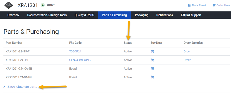
Parts & Purchasing
| Part Number | Pkg Code | Min Temp | Max Temp | Status | Suggested Replacement | Buy Now | Order Samples | PDN |
|---|---|---|---|---|---|---|---|---|
| XR16V554IJ-F | PLCC68 | -40 | 85 | OBS | ST16C554DIJ68-F | |||
| XR16V554IJTR-F | PLCC68 | -40 | 85 | OBS | XR16V554IJ-F | |||
| XR16V554IL-F | QFN48 7x7 | -40 | 85 | OBS | XR16M654IL48-F | |||
| XR16V554ILTR-F | QFN48 7x7 | -40 | 85 | OBS | XR16V554IL-F | |||
| XR16V554IV | LQFP64 | -40 | 85 | OBS | ||||
| XR16V554IV-F | LQFP64 | -40 | 85 | Active | Order | |||
| XR16V554IV80-F | LQFP80 12x12 | -40 | 85 | OBS | XR16V654IV80-F | |||
| XR16V554IV80TR-F | LQFP80 12x12 | -40 | 85 | OBS | XR16V554IV80-F | |||
| XR16V554IVTR-F | LQFP64 | -40 | 85 | OBS | XR16V554IV-F |
Active - the part is released for sale, standard product.
EOL (End of Life) - the part is no longer being manufactured, there may or may not be inventory still in stock.
CF (Contact Factory) - the part is still active but customers should check with the factory for availability. Longer lead-times may apply.
PRE (Pre-introduction) - the part has not been introduced or the part number is an early version available for sample only.
OBS (Obsolete) - the part is no longer being manufactured and may not be ordered.
NRND (Not Recommended for New Designs) - the part is not recommended for new designs.
Packaging
Notifications
FAQs & Support
Search our list of FAQs for answers to common technical questions.
For material content, environmental, quality and reliability questions review the Quality tab or visit our Quality page.
For ordering information and general customer service visit our Contact Us page.
Submit a Technical Support Question As a New Question
https://www.exar.com/quality-assurance-and-reliability/lead-free-program
The Parts & Purchasing section of the product page shows the Status of all orderable part numbers for that product. Click Show obsolete parts, to see all EOL or OBS products.
Please check that all the following conditions are satisfied first.
- no interrupts pending (ISR bit-0 = 1)
- modem inputs are not toggling (MSR bits 0-3 = 0)
- RX input pin is idling HIGH • divisor (the value in DLL register) is non-zero
- TX and RX FIFOs are empty
Be sure sleep mode bit has been set to 1. If there are multiple UART channels, the sleep conditions must be true for all channels.
See more on Sleep Mode in AN204 UART Sleep Mode.
Yes. Note: some devices do have powersave mode. If UART goes into powersave mode, then the registers are not accessible.
See more on Sleep Mode in AN204 UART Sleep Mode.
Read LSR register to check whether the UART receives the data or not.
- If LSR value is 0x60, it means that either UART receiver FIFO doesn’t receive the data or the data in receiver FIFO has been read out before the read of LSR.
- If LSR value is 0x00, it means data is still in the THR (clock doesn’t oscillate to transmit data).
- If LSR value is 0xFF, it means either UART is in powersave mode or UART is powered off. For those devices with powersave mode, be sure that UARTS are not in powersave mode.
See more on Sleep Mode in AN204 UART Sleep Mode.
- Check whether the register set can be accessed.
- Check whether the crystal is oscillating fully.
- Check whether the data can be transmitted in internal loopback mode.
See more on Sleep Mode in AN204 UART Sleep Mode.