Overview
| Information | 35A Synchronous Step- Down COT Controller |
|---|---|
| Max Rec. Output Current (A) | 35 |
| IQ (µA) | 700 |
| VIN MIN (V) | 3 |
| VIN MAX (V) | 22 |
| VOUT MIN (V) | 0.6 |
| VOUT MAX (V) | 18 |
| Frequency (kHz) | 200-800 |
| Efficiency (%) | 95 |
| Control Mode | Proprietary emulated current mode COT |
| Special Features | Light Load PFM, Enable, Power Good, Power Sequencing, Synchronous Rectification, Thermal Shutdown, UVLO, Internal 5V VCC, Soft Start Adjustable |
| Operating Temp Range (°C) | -40 to 125 |
| Package | QFN-16 |
The XRP6141 is a synchronous step-down controller for point-of load supplies up to 35A. A wide 4.5V to 22V input voltage range allows for single supply operation from industry standard 5V, 12V and 19.6V rails.
With a proprietary emulated current mode Constant On-Time (COT) control scheme, the XRP6141 provides extremely fast line and load transient response using ceramic output capacitors. It requires no loop compensation hence simplifying circuit implementation and reducing overall component count. The control loop also provides exceptional line regulation and maintains constant operating frequency. A selectable power saving mode, allows the user to operate in Discontinuous Mode (DCM) at light current loads thereby significantly increasing the converter efficiency.
A host of protection features, including overcurrent, over temperature, short-circuit and UVLO, help achieve safe operation under abnormal operating conditions.
The XRP6141 is available in RoHS compliant, green/halogen free space-saving 16-pin 3 x 3 QFN package.
- 35A capable step-down controller
- Wide input voltage range
- 5V to 22V single supply
- 4.5V to 5.5V low VIN
- Integrated high current 2A/3A drivers
- 0.6V adjustable output voltage
- Wide input voltage range
- Proprietary constant on-time control
- No loop compensation required
- Ceramic output cap. stable operation
- Programmable 200ns-2µs
- Constant 200kHz-800kHz Frequency
- Selectable CCM or CCM/DCM operation
- Programmable current limit
- 110ms hiccup mode
- Precision enable and power good flag
- Programmable soft-start
- Integrated bootstrap diode
- 16-pin QFN packages
- Networking and communications
- Fast transient point-of-loads
- Industrial and medical equipment
- Embedded high power FPGA
- Enterprise solutions
Documentation & Design Tools
| Type | Title | Version | Date | File Size |
|---|---|---|---|---|
| Data Sheets | XRP6141 35A Synchronous Step Down COT Controller | Rev. 2.0.3.2 | November 2019 | 1.1 MB |
| Application Notes | AN200, Downloading and Installing CAD Symbols and Footprints with Ultra Librarian | April 2019 | 1.2 MB | |
| User Guides & Manuals | XRP6141 Evaluation Board User Manual | 1.0.0 | November 2013 | 1.5 MB |
| Product Brochures | Power Management Brochure | October 2020 | 2.4 MB | |
| Symbols & Footprints | XRP6141EL-F CAD File (.bxl) | September 2018 | 134.2 KB | |
| Symbols & Footprints | XRP6141ELTR-F CAD File (.bxl) | September 2018 | 134.2 KB | |
| Schematics & Design Files | XRP6141EVB CAD Files | 1.0.0 | January 2014 | 52.1 KB |
Quality & RoHS
Parts & Purchasing
| Part Number | Pkg Code | Min Temp | Max Temp | Status | Suggested Replacement | Buy Now | Order Samples | PDN |
|---|---|---|---|---|---|---|---|---|
| XRP6141EL-F | QFN16 3x3 | -40 | 125 | OBS | XRP6141ELTR-F | |||
| XRP6141ELMTR-F | QFN16 3x3 | -40 | 125 | OBS | XRP6141ELTR-F | |||
| XRP6141ELTR-F | QFN16 3x3 | -40 | 125 | Active | Order | |||
| XRP6141EVB | Board | Active |
Active - the part is released for sale, standard product.
EOL (End of Life) - the part is no longer being manufactured, there may or may not be inventory still in stock.
CF (Contact Factory) - the part is still active but customers should check with the factory for availability. Longer lead-times may apply.
PRE (Pre-introduction) - the part has not been introduced or the part number is an early version available for sample only.
OBS (Obsolete) - the part is no longer being manufactured and may not be ordered.
NRND (Not Recommended for New Designs) - the part is not recommended for new designs.
Packaging
Notifications
FAQs & Support
Search our list of FAQs for answers to common technical questions.
For material content, environmental, quality and reliability questions review the Quality tab or visit our Quality page.
For ordering information and general customer service visit our Contact Us page.
Submit a Technical Support Question As a New Question
The Exar controllers, regulators and power modules are powered by an internal LDO to produce the Vcc rail that their circuits need to run properly. If the input voltage that feeds the LDO is the minimum Vin as specified on the datasheet or above, the Vcc is enough to power the device and the Vin, Vcc and PVIN pins can be connected together.
If the input voltage is 5V, then the Vin and Vcc pins can be tied together and the input voltage is fed to the PVIN pin.
If input voltage is below 5V, then a separate low current 5V supply (common in many systems) is connected to the Vin and Vcc pins which are tied together to keep the device running properly. The input voltage is connected to the PVIN pin.
Voltage mode PWM
Voltage mode PWM is a simple technique that uses a single loop to control the output voltage. As shown in Figure 1, the output voltage is compared to a reference voltage with an error amplifier. The output of the error amplifier is then compared to a sawtooth and that output is used to drive the MOSFET, usually via a voltage divider.
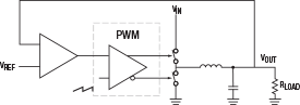
Figure 1
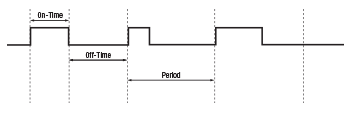
As shown in Figure 2, the output voltage is modulated by turning the high-side FET on (on-time) with the pulse width and turning the low side FET off. At the end of the pulse, the high-side FET is turned off (off-time) and the low side FET is turned on until the next pulse. Vout = On-Time/Period * Vin.
The advantages of voltage mode PWM is that it is a very simple, common, smaller solution with good accuracy. The disadvantages are that complex frequency compensation is required (two poles) to stabilize the loop and because trailing edge control is most commonly used, there is a delay in load step response.
Current mode PWM
With voltage mode PWM, current is less known. For better control, current mode PWM senses the inductor current and it is compared to the reference voltage as shown in Figure 3.
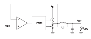
Figure 3
Although the current has to be sensed with accuracy and introduces noise, the advantages of current mode PWM are easier loop compensation (less compensation needed with one pole), and it is easier to implement over-current protection and parallel currents to the output.
Standard Constant On-Time (COT)
As opposed to PWM, the pulse width in COT is always the same as shown in Figure 4. Instead the off-time length varies (as does the frequency) which modulates the output. As the Vout increases, the off-time of the duty cycle increases (frequency decreases) and the fixed on-time produces a lower duty cycle. This transfers less energy to the output and lowers the Vout. More simply said, as Vout increases, the duty cycle decreases. Conversely, as the Vout decreases, the off-time of the duty cycle decreases (frequency increases) and the fixed on-time produces a higher duty cycle. This transfers more energy to the output and raises the Vout.
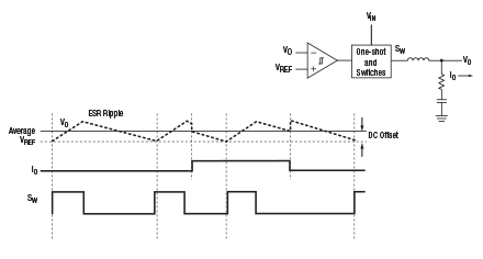
Figure 4
The advantages of standard COT are very fast transient response, simplicity (inexpensive) and that frequency compensation is not complex as it is in PWM control. However, the feedback signal tends to have low amplitude and signal to noise ratio, making it very noise sensitive. Also, the output voltage is higher than the reference voltage and the ripple is dependent on and sensitive to the output capacitor ESR. This introduces a DC offset which is the average amount the output voltage is over the reference voltage. It is also jitter prone and the frequency changes during the load steps.
Some solutions solve the noise sensitivity by having one of two options that condition the feedback signal but introduce delays. One tradeoff provides faster transient responses; the other allows low ESR output capacitors to be used.
MaxLinear’s patented COT
MaxLinear’s patented COT architecture however conditions the reference instead as shown in Figure 5. The MaxLinear devices create their own emulated ramp that is insensitive to noise and the ESR of the capacitor. Since the output capacitor ESR does not affect it, low ESR ceramic capacitors can be used and maintain stability without decreasing speed. In addition, the Vout and reference voltage are compared and that result controls the ramp circuit. This creates a slower loop where the output voltage is averaged out and the DC offset is not introduced as in standard COT.
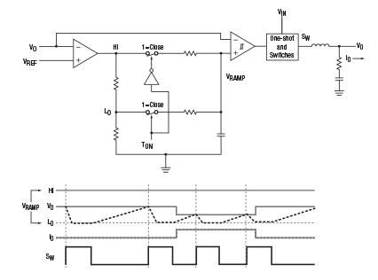
Figure 5
MaxLinear’s COT still has the standard COT advantages of very fast transient response, simplicity and no complex frequency compensation in addition to not having DC offset or ESR value sensitivity. MaxLinear’s COT architecture provides exceptional line and load regulation.
Find the product page of the part that you want to get an evaluation board for and click on Parts & Purchasing. Example:
Find the icons under Buy Now or Order Samples:
Click on the Buy Now icon and see who has stock and click on the Buy button:
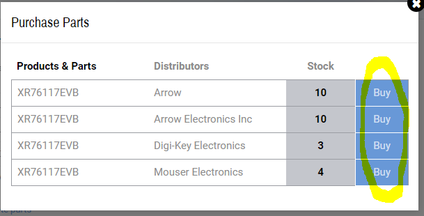
Alternatively, you can click on the Order Samples
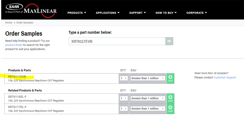
If the icons are missing, then contact Customer Support.
In PWM controllers, frequency is constant and tON (on-time) is set by the controller to regulate the output voltage. However in COT controllers, the tON is constant and set by the RON resistor. This also sets the frequency. RON is connected between the TON pin and GND.
If the high-side FET was ideal, the tON of the SW signal would be equal to tON of GH (high-side FET gate) signal and the relationship between RON and tON would be:
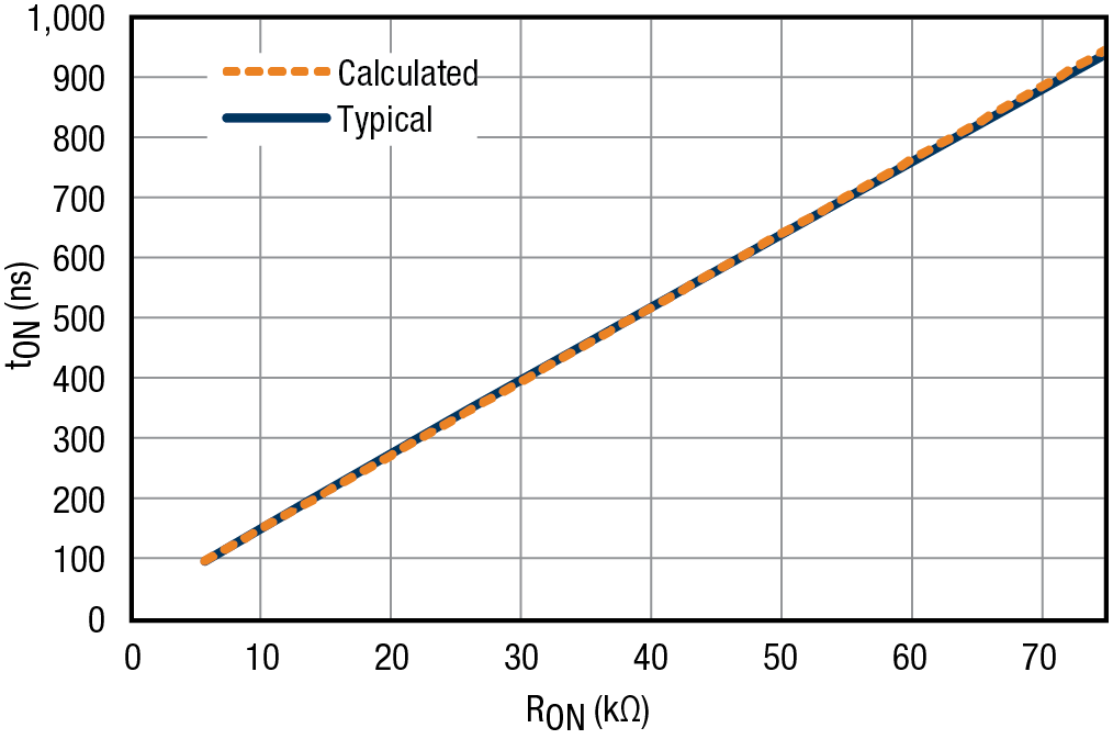
However, the high side FET has rise and fall times as well as on and off delay times, so the tON of SW is not equal to GH. This non-ideal characteristic is measured for each regulator or module where the above equation is modified. In the Applications Information of each regulator or module datasheet, an equation defining the relationship of RON and tON is given based on test data for that device. For example, in the XR79206 power module datasheet, you will find the following equation in the Programming the On-Time section of the Applications Information:
The correlation of this equation to the test data is also given in the datasheet. In the XR79206 example, Figure 5 in the Typical Performance Characteristics section shows very good correlation:
However, as no Buck Converter is ideal, test data is taken to determine a more accurate equation which is also given in the datasheet. In the XR79206 example, the following equation is given based on test data:
Substituting this tON equation into the above equation relating RON and tON and simplifying, we get:
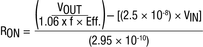
Then RON can be easily chosen based on the targeted VIN, VOUT, frequency and efficiency. So for example in the XR79206, if VIN = 24V, VOUT = 5V, f = 500kHz and efficiency = 90%,

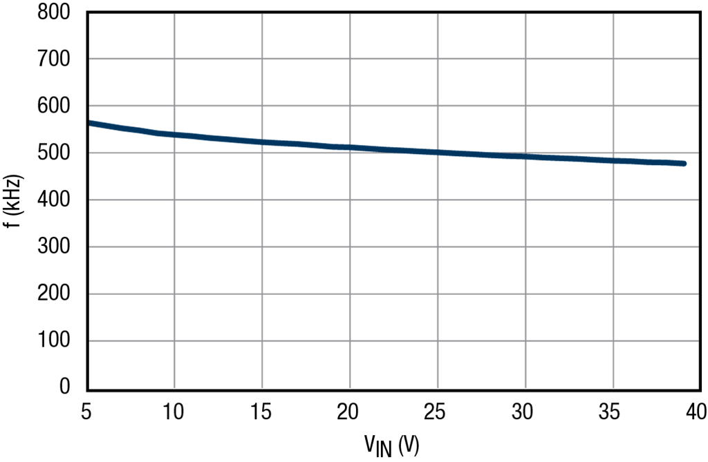
As IOUT increases, frequency increases slightly due to increasing power losses. As losses increase, more power must be delivered per cycle to keep VOUT constant. Because tON is constant, the period decreases and frequency increases, as can be seen in the following example from the XR79206 datasheet:

https://www.exar.com/quality-assurance-and-reliability/lead-free-program

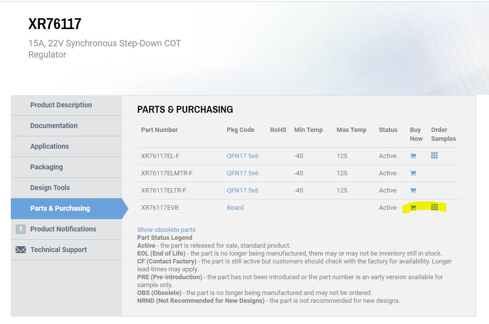
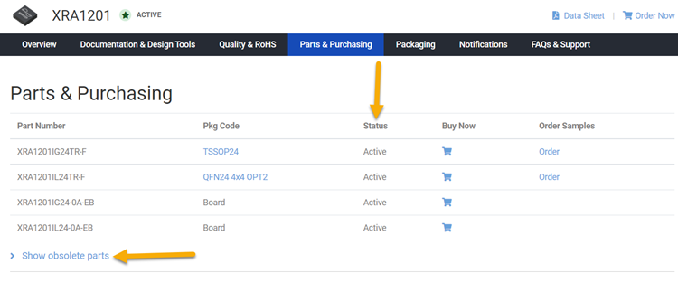
The Parts & Purchasing section of the product page shows the Status of all orderable part numbers for that product. Click Show obsolete parts, to see all EOL or OBS products.
The COT families (XRP6141, XRP6124 and XR75100 controllers, XR76xxx regulators and XR79xxx power modules) have 2 modes of operation that can be set: DCM / CCM (discontinuous conduction mode / continuous conduction mode) or FCCM (Forced CCM) mode. In FCCM mode, the converter operates at a preset frequency regardless of output current. In DCM / CCM mode the converter operates in DCM or CCM depending on the Iout magnitude. If Iout < ½ Ipp, the converter transitions to DCM mode. If Iout is higher, operation is in CCM mode.
The main advantage of DCM / CCM is that it provides significantly higher efficiency at light loads. For those applications where that doesn’t matter, FCCM can be used and has the advantage that it allows for operation at a constant frequency, regardless of load. It also results in lower Vout ripple, and will operate in an inaudible range.
There are many factors to consider in selecting the inductor including core material, inductance versus frequency, current handling capability, efficiency, size and EMI. Typically, the inductor is primarily chosen for value, saturation current and DC resistance (DCR). Increasing the inductor value will decrease output voltage ripple, but degrade transient response. Low inductor values provide the smallest size, but cause large ripple currents, poor efficiency and require more output capacitance to smooth out the larger ripple current. The inductor must be able to handle the peak current at the switching frequency without saturating, and the copper resistance in the winding should be kept as low as possible to minimize resistive power loss. A good compromise between size, loss and cost is to set the inductor ripple current to be within 20% to 40% of the maximum output current.
The switching frequency and the inductor operating point determine the inductor value as follows:
L = Vout x (Vinmax – Vout) / Vinmax x fs x Kr x Ioutmax
Where fs = switching frequency
Kr = ratio of the AC inductor ripple current to the maximum output current
So for example, we want to choose L for the XR76108 (Ioutmax 8A) and wish to convert 12Vin to 2.5Vout with a frequency of 1MHz:
In our example, Ipp = 35% x 8A = 2.8A
Once the required inductor value is selected, the proper selection of core material is based on peak inductor current and efficiency requirements. The core must be large enough not to saturate at the peak inductor current.
Ipeak = Ioutmax + Ipp/2
In our example, Ipeak = 8A + 2.8A/2 = 9.4A
In general, it is set for Imax x 1.5. It would be close the maximum Iout (including ripple). If conservatively set too high, the hiccup mode may not be activated fast enough. If set too low, the ripple could cause the current to go over the threshold and set it into hiccup on a pre-mature basis.
A zero-cross comparator monitors the voltage across the low-side FET when it is on. The comparator threshold is nominally set at -1mV or -2mV (see individual datasheet). If there is sufficient IOUT such that VSW is below the threshold and therefore does not trigger the zero-cross comparator, CCM operation continues.
As IOUT is reduced, VSW gets closer to ground. When VSW meets the threshold, the zero-cross comparator triggers. If there are 8 consecutive triggers, then DCM operation begins. The low side FET is turned off when IL x RDS equals the zero-cross threshold.
As there is no negative inductor current, the charge transferred to COUT is preserved. As IOUT decreases further, less charge transfer to COUT is required. Pulses grow further apart, frequency is reduced and efficiency increases.
DCM persists as long as there are 8 consecutive zero-crosses.
Note that when the DCM frequency falls below about 1kHz, the controller turns on the lower-side FET for 100ns once every 1.2ms to refresh the charge on the bootstrap capacitor. This refresh cycle generates small spikes on SW, which can be seen interlaced between DCM pulses.