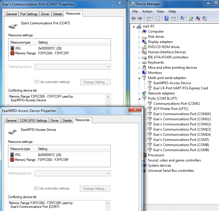
Frequently Asked Questions

The Exar controllers, regulators and power modules are powered by an internal LDO to produce the Vcc rail that their circuits need to run properly. If the input voltage that feeds the LDO is the minimum Vin as specified on the datasheet or above, the Vcc is enough to power the device and the Vin, Vcc and PVIN pins can be connected together.

If the input voltage is 5V, then the Vin and Vcc pins can be tied together and the input voltage is fed to the PVIN pin.

If input voltage is below 5V, then a separate low current 5V supply (common in many systems) is connected to the Vin and Vcc pins which are tied together to keep the device running properly. The input voltage is connected to the PVIN pin.

Voltage mode PWM

Voltage mode PWM is a simple technique that uses a single loop to control the output voltage. As shown in Figure 1, the output voltage is compared to a reference voltage with an error amplifier. The output of the error amplifier is then compared to a sawtooth and that output is used to drive the MOSFET, usually via a voltage divider.
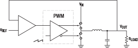


Figure 1


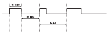
As shown in Figure 2, the output voltage is modulated by turning the high-side FET on (on-time) with the pulse width and turning the low side FET off. At the end of the pulse, the high-side FET is turned off (off-time) and the low side FET is turned on until the next pulse. Vout = On-Time/Period * Vin.


Figure 2
 

The advantages of voltage mode PWM is that it is a very simple, common, smaller solution with good accuracy. The disadvantages are that complex frequency compensation is required (two poles) to stabilize the loop and because trailing edge control is most commonly used, there is a delay in load step response.

Current mode PWM

With voltage mode PWM, current is less known. For better control, current mode PWM senses the inductor current and it is compared to the reference voltage as shown in Figure 3.
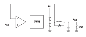


Figure 3


Although the current has to be sensed with accuracy and introduces noise, the advantages of current mode PWM are easier loop compensation (less compensation needed with one pole), and it is easier to implement over-current protection and parallel currents to the output.

Standard Constant On-Time (COT)

As opposed to PWM, the pulse width in COT is always the same as shown in Figure 4. Instead the off-time length varies (as does the frequency) which modulates the output. As the Vout increases, the off-time of the duty cycle increases (frequency decreases) and the fixed on-time produces a lower duty cycle. This transfers less energy to the output and lowers the Vout. More simply said, as Vout increases, the duty cycle decreases. Conversely, as the Vout decreases, the off-time of the duty cycle decreases (frequency increases) and the fixed on-time produces a higher duty cycle. This transfers more energy to the output and raises the Vout.
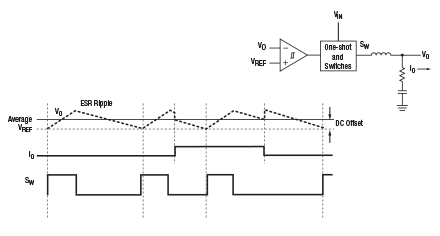


Figure 4


The advantages of standard COT are very fast transient response, simplicity (inexpensive) and that frequency compensation is not complex as it is in PWM control. However, the feedback signal tends to have low amplitude and signal to noise ratio, making it very noise sensitive. Also, the output voltage is higher than the reference voltage and the ripple is dependent on and sensitive to the output capacitor ESR. This introduces a DC offset which is the average amount the output voltage is over the reference voltage. It is also jitter prone and the frequency changes during the load steps.

Some solutions solve the noise sensitivity by having one of two options that condition the feedback signal but introduce delays. One tradeoff provides faster transient responses; the other allows low ESR output capacitors to be used.

MaxLinear’s patented COT

MaxLinear’s patented COT architecture however conditions the reference instead as shown in Figure 5. The MaxLinear devices create their own emulated ramp that is insensitive to noise and the ESR of the capacitor. Since the output capacitor ESR does not affect it, low ESR ceramic capacitors can be used and maintain stability without decreasing speed. In addition, the Vout and reference voltage are compared and that result controls the ramp circuit. This creates a slower loop where the output voltage is averaged out and the DC offset is not introduced as in standard COT.
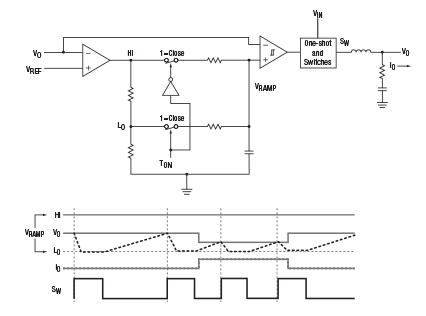


Figure 5


MaxLinear’s COT still has the standard COT advantages of very fast transient response, simplicity and no complex frequency compensation in addition to not having DC offset or ESR value sensitivity. MaxLinear’s COT architecture provides exceptional line and load regulation.

The XR76117 and XR76121 are identical to each other except for their output current rating. Similarly the IR3824/IR3825/IR3829 are identical to each other except for the differences shown in this section. Output current ratings are summarized in Table 1.


Spec

Exar XR76117 / XR76121

Infineon IR3824 / IR3825 / IR3829

Max IOUT

15A (XR76117); 20A (XR76121)

15A (IR3824); 16A (IR3829); 20A (IR3825)

VIN range

4.5V to 22V

5V to 21V

VOUT range

0.6V to 18V

0.6V to 0.86 x VIN

Frequency range

200kHz to 1MHz

Up to 1.5MHz

Temperature range

-40°C to 125°C

-40°C to 125°C

Supply current

17mA

20mA


Table 1: Major Specification Comparison 
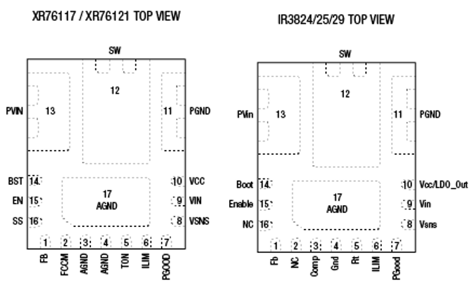
 
The XR76117 / XR76121 can be soldered into a IR3824/25/29 socket, only minor board stuff options are required. The following and Application Note ANP-49 discuss how both series can occupy the same socket on a PCB.


Pin-out comparison


Figure 1: Pin-out Comparison 
 

Pin

XR76117 / XR76121

IR3824 / IR3825 / IR3829

Same

Function /

Connection?

Changes Required to Drop XR76117/21 into IR3824/25/29 Socket

1

FB

Fb

Yes/Yes

None

2

FCCM

NC

No/No

Must either be tied to VCC for FCCM operation or tied to GND for CCM/DCM operation. Pull-up or pull-down resistors may also be used. See Figure 2 and XR76117 or XR761121 datasheet for more information.

3

AGND

Comp

No/No

Add a 0Ω resistor to jumper pin 3 to pin 4 and do not stuff compensation Cs/Rs. Refer to Figure 2.

4

AGND

Gnd

Yes/Yes

None

5

TON

Rt

No/Yes

In both cases, this pin sets frequency and requires a resistor to GND. However, a different resistor value must be used for the XR solution. Refer to the XR76117 / XR76121 datasheet for resistor value calculation.

6

ILIM

ILIM

Yes/No

Add a 0Ω resistor to connect to SW. Do not stuff resistors to VCC or GND. Refer to Figure 2.

7

PGOOD

PGood

Yes/Yes

None

8

VSNS

Vsns

Yes/Yes

None

9

VIN

Vin

Yes/Yes

None

10

VCC

Vcc/

LDO_Out

Yes/Yes

None

11

PGND

PGnd

Yes/Yes

None

12

SW

SW

Yes/Yes

None

13

PVIN

PVin

Yes/Yes

None

14

BST

Boot

Yes/Yes

None

15

EN

Enable

Yes/Yes

None

16

SS

NC

No/No

Add an external capacitor to GND. See Figure 2 or the XR76117/XR76121 datasheet for more information.

17

AGND PAD

GND

Yes/Yes

None


Table 2: Pin-out Comparison & Changes Required to Drop XR76117 / XR76121 into IR3824 / IR3825 / IR3829 Socket 

 
Board Stuff Option Schematic
 

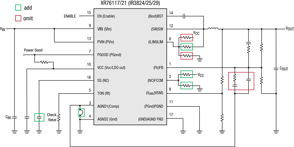
The PCB board can be easily designed to drop-in the XR76117 or XR76121 while maintaining compatibility to the IR3824/25/29. In Figure 2 below, pinning for both series are represented. The Exar XR76117 and XR76121 pin names do not have parenthesis, and the same corresponding pins for the IR3824/25/29 are in parenthesis. As shown in the legend, the components in green boxes are added and the ones in red boxes are omitted when using the XR76117 or XR76121. Both a pull-up and pull-down are shown for pins 2 and 6, but only one or the other will be present depending on the application. So, 4 passives (red) will not be populated while 3 passives and a jumper will be populated.


Figure 2: Addition and Omission of External Components 
 

With a plethora of equipment with built in USB ports, USB hubs assist by expanding the number of USB ports available to plug devices into in a network. In its simplest form, a USB hub is plugged into a host computer’s USB interface. A hub has one upstream path (going back towards the host’s USB interface) and multiple downstream paths (going towards the end devices). Another downstream hub could be plugged and cascaded into the first hub and so on up to 7 tiers and 127 ports. There are limitations on USB cable length, however a USB hub can function as a repeater if more length is needed.  See AN213 section 3.0 for more information.


USB is governed by industry specification http://www.usb.org/developers/docs/usb20_docs/ .


MaxLinear XR22404 and XR22414 USB hubs have 4 available downstream ports while the XR22417 provides 7. All 3 parts have a USB 2.0 compliant interface, meaning that the upstream is capable of high speed (480Mbps) and may operate at high (480Mbps) or full speed (12Mbps). Downstream can operate and high (480Mbps), full (12Mbps) or low speed (1.5Mbps).


USB 2.0 host ports provide up to 5 unit loads of 100 mA per attached peripheral device (including USB hubs). A bus powered hub, powered from USB host 5 volt VBUS, can supply a maximum of 1 unit load on each of its downstream ports. For example, a 4-port hub must be able to supply 4 x 100 mA or 400 mA total and is also allotted 100 mA for its own power requirements. A hub with more than 4 downstream ports cannot be bus powered.

Conversely, a self-powered hub is powered by an outside power source. It is restricted in the number of downstream ports and the power to those ports only by the power from the external source. A self-powered hub should typically be able to provide a minimum of 5 unit loads per downstream port.

MaxLinear has a number of USB 2.0 hub products. The 4-port XR22404, XR22414 and 7-port XR22417 all support self-powered mode while XR22404 and XR22414 can also be bus-powered. The XR22404 can provide battery charging on its downstream ports, but must be in self-powered mode to do so.

 
For more on USB Basics, see Application Note AN213 for more. 


 A transaction translator (TT) segregates and translates between high speed (USB 2.0 / 480Mbps) upstream ports and USB 1.1 downstream ports. USB 1.1 can be low speed (1.5Mbps) or full speed (12Mbps). USB 2.0 devices operate at full or high speed, and compliant USB 2.0 hubs have high speed capable upstream ports like the XR22404, XR22414 and XR22417. Downstream ports may be high, full or low speed. When a USB 1.1 device is plugged into a USB 2.0 hub, the TT recognizes this and translates USB 1.1 to USB 2.0 upstream.
 

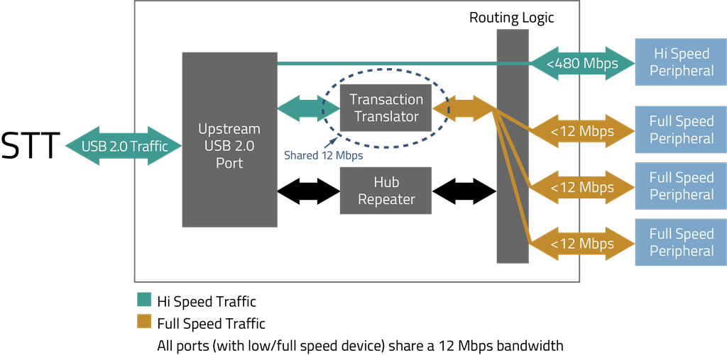
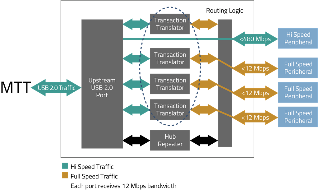
STT (Single Transaction Translator) is where one TT splits transactions and polls round robin to translate to multiple downstream peripheral devices, such as in the case of the XR22404 that shares the bandwidth. MTT (Multiple Transaction Translator) is where several are provided. The XR22414 provides one for each of the 4 downstream ports, while the XR22417 provides one for each of the 7 downstream ports. A dedicated TT for the downstream ports provides each the highest bandwidth capability, 12Mbps each in the case of full speed.


Either an individual or ganged power mode can be employed. In ganged mode all ganged ports are monitored by one power monitoring device and global current sensing is used. However in an over-current condition, all ganged ports are disabled. In individual mode each downstream port monitors over-current and can disable power independently. XR22404 uses ganged power mode and global overcurrent sensing. XR22414 can be configured for either ganged or individual power mode as shown in its datasheet. XR22417 uses individual power mode.


The hub then signals the USB host and the host marks the port. SP2525A or SP2526A can be used in conjunction with the XR22404, XR22414 and XR22417 devices.

For some UARTs, Microsoft certified drivers are available for Windows Operating System and can be downloaded via Windows Update. These drivers and others, including for Linux and other Operating Systems can be found by visiting https://www.exar.com/design-tools/software-drivers Please note Software Driver Use Terms.


You can also get to this link by going to the exar.com website, clicking on Support (in black bar near top of page), then click on Design Tools, then under Evaluation Hardware and Software (towards right of page) click on Software Drivers.


Click on the version link under Driver Version of the desired type of UART, part number and operating system. A zip file is downloaded which contains a ReadMe file with instructions.

Links to datasheets and product family pages are in the software driver table for easy reference. 

For RS-232 it is 50 feet (15 meters), or the cable length equal to a capacitance of 2500 pF, at a maximum transmission rate of 19.2kbps. When we reduce the baud rate, it allows for longer cable length. For Example:


Baud Rate (bps)

Maximum RS-232 Cable Length (ft)

19200

50

9600

500

4800

1000

2400

3000

 
For RS-485 / RS-422 the data rate can exceed 10Mbps depending on the cable length. A cable length of 15 meters (50 feet) will do a maximum of 10Mbps. A cable length of 1200 meters (4000 feet) will do a maximum of 90kbps over 24 AWG gauge twisted pair cable (with 10 pF/ft). Refer to Annex A TIA/EIA-422-B. Also refer the RS-485 Cable Lengths vs. Data Signaling Rate Application Note (AN-292).
 
 
As RS-422/RS-485 uses differential signaling, it is more immune to noise and longer cables and/or high data rates can be used, especially in noisy environments. Also, RS-485 allows for multi-point operation, up to 32 unit loads. Transceivers may use a fraction of a unit load, increasing the number of devices on the bus. For example, the XR33152 receiver input impedance is at least 120 k, which equates to 1/10 of a unit load. Therefore, XR33152 allows more than 320 devices (32 x 10) on the bus.

Fail Safe is an attempt to keep the output of the RS-485 receiver to a known state. Transceivers may have standard fail safe or advanced / enhanced receiver fail safe features. Standard fail safe supports open inputs while enhanced fail safe transceivers such as the SP339 and XR34350 support open input, shorted input and undriven terminated lines without external biasing. See Application Note ANI-22 for more detail.


Figure 1:  Standard Failsafe Receiver Sensitivity Range


Figure 2: Standard Failsafe with Open Input


Figure 3: Enhanced Failsafe Receiver Sensitivity Range


Figure 4:  Enhanced Failsafe with Open Input


Figure 5:  Enhanced Failsafe with Shorted Input


Figure 6:  Enhanced Failsafe with Un-driven terminated lines


The XR17Cxxx, XR17Dxxx, and XR17Vxxx are all UARTs but have the following basic differences:

  • PCI UARTs
    • XR17Cxxx – 5V supply, up to 33MHz clock input
    • XR17Dxxx – 5V or 3.3V supply, up to 33MHz clock input
    • XR17V2xx – 3.3V supply, up to 66MHz clock input
  • PCIe UARTs
    • XR17V3xx – 3.3V supply, up to 125MHz clock input
Yes, however, you will need to use a PCI-PCI bridge.
The schematics for our evaluation boards are available for download from https://www.exar.com/technical-documentation?doctypeid=34
No, it is not required. If an external EEPROM is not detected, the PCI UARTs will use Exar's default Vendor and Device ID. However, we do recommend that you use an EEPROM with your own Vendor and Device IDs.
You will need to be a member of PCI-SIG. You can find information for becoming a member at www.pcisig.com.
Typically, this device will be used in an application with a microcontroller that has either an SPI or I2C interface. There should already be some sample code for communicating with a device on the I2C or SPI bus. The microcontroller will just need to provide the appropriate address or CS# to communicate with the I2C/SPI UART.
There is a pin to select between the I2C and the SPI mode. The pin is connected to VCC to select the I2C mode and connected to GND to select the SPI mode.
By default, the GPIOs are in the input state so they must be connected to VCC or GND, or they must be set as outputs after power-up. If they are set as outputs after power-up, then there will be extra current as the GPIOs are floating.
Our evaluation boards have the UART, a transceiver (RS-232, RS-485/422 or IR), a connector for the transceiver, and some test points for either the I2C or the SPI signals to interface directly with a microcontroller with an I2C or an SPI interface.
LSR bit-6 is a superset of LSR bit-5. The transmitter consists of a TX FIFO (or THR only when FIFOs are not enabled) and a Transmit Shift Register (TSR). When LSR bit-5 is set, it indicates that the TX FIFO (or THR) is empty, however there may be data in the TSR. When LSR bit-6 is set, it indicates that the transmitter (TX FIFO + TSR) is completely empty.
You can tell by reading LSR bit-5 or bit-6. If they are '0', then the transmit interrupt was generated by the trigger level. If they are '1', then the transmit interrupt was generated by the TX FIFO becoming empty. For enhanced UARTs, you can just read the FIFO level counters.
An RX Data Ready interrupt is generated when the number of bytes in the RX FIFO has reached the RX trigger level. An RX Data Timeout interrupt is generated when the RX input has been idle for 4 character + 12 bits time.
For some UARTs, the RX Data Timeout interrupt has a higher priority and in others, the RX Data Ready interrupt has a higher priority. See the interrupt priority section of the datasheet.
The UART requires a clock and a valid baud rate in order to transmit and receive data. Check that there is a clock signal on the XTAL1 input pin. Also, valid divisors need to be written into the DLL and DLM registers. Most UARTs have random (invalid) values upon power-up.
For most UARTs, the interrupt is generated when the data is ready to be read from the RX FIFO. The are some UARTs that generate the interrupt when the character with the error is received. There are some UARTs that have a register bit to select whether the LSR interrupt is generated immediately or delayed until it is ready to be read.
The UART will enter the sleep mode if the following conditions have been satisfied for all channels:
 
-Sleep Mode is enabled
-No interrupts are pending
-TX and RX FIFOs are empty
-RX input pin is idling HIGH (LOW in IR mode)
-Valid values in DLL and DLM registers
-Modem input pins are idle (MSR bits 3-0=0x0)
 
See AN204, UART Sleep Mode for more information on UART Sleep Mode
The UART will wake-up from sleep mode by any of the following conditions on any channel:
 
-Sleep mode is disabled
-Interrupt is generated
-Data is written into THR
-There is activity on the RX input pin
-There is activity on the modem input pins
 
If the sleep mode is still enabled and all wake-up conditions have been cleared, it will return to the sleep mode.
 
See AN204, UART Sleep Mode for more information on UART Sleep Mode 
There will be no activity on the XTAL2 output.
 
See AN204, UART Sleep Mode for more information on UART Sleep Mode 
For any UART that has the wake-up indicator interrupt, an interrupt will be generated when the UART wakes up even if no other interrupts are enabled.
 
See AN204, UART Sleep Mode for more information on UART Sleep Mode 
No, Auto RTS and Auto CTS are independent. Auto RTS is toggled by the UART receiver. Auto CTS is monitored by the UART Transmitter.
No, Auto RTS and Auto CTS will work normally without the interrupts enabled.
No, software flow control characters are not loaded into the RX FIFO.
Since 2-character software flow control requires that 2 consecutive flow control characters match before data transmission is stopped or resumes, there is less of a chance that data transmission is stopped because one data byte matched a control character.
Auto RS485 Half-Duplex Control feature overrides the Auto RTS flow control feature if both features use the RTS# output pin. Both features can only be used simultaneously if the Auto RS485 control output is not the RTS# output. For some UARTs, the Auto RS485 control output is not the RTS# output.
Most UARTs use RTS#, however the XR16C850 and XR16C864 use the OP1# output as the Auto RS485 control output. In addition to using the RTS# output as the Auto RS485 control output, the XR16L784, XR16L788 and XR16V798 can use the DTR# output as the Auto RS485 control output.
The polarity of the RS485 control output varies from one UART to another. For some UARTs, an inverter may be required. Some of the newer UARTs have register bits that can change that polarity of the RS485 control output.
In the normal mode, the TX interrupt is generated when the TX FIFO is empty, and there may still be data in the Transmit Shift Register. In the RS485 mode, the TX interrupt is generated when the TX FIFO and the TSR register are both empty.
It is recommended that the FIFO counters at the Scratchpad Register location be used. When transmitting or receiving data, writing to the LCR register could result in transmit and/or receive data errors.
Due to the dynamic nature of the FIFO counters, it is recommended that the FIFO counter registers be read until consecutive reads return the same value.
All of the UARTs that have the IR mode supports up to 115.2Kbps as specified in IrDA 1.0. The newer I2C/SPI UARTs can support up to 1.152Mbps as specified in IrDA 1.1.
For external clock frequencies above 24MHz at the XTAL1 input, a 2K pull-up may be necessary to improve the rise times if there are data transmission errors.
Yes, you can daisy-chain it like that, but only up to 2 times (3 UARTs total in the daisy-chain). The UARTs should be as close as possible.
Yes, if you are using a UART with a fractional baud rate generator. This provides a divisor feature with a granularity of 1/16, allowing for any baud rate to be generated by any clock frequency, standard or non-standard. Click on the parametric search button of the product family page and find the Fractional Baud Rate Generator column which tells which products have this feature.
They crystal oscillator circuitry is recommended for fundamental frequency crystals only. The maximum frequency for crystals with fundamental frequencies is typically 24MHz. Above that frequency, crystals operate at higher harmonics, which will not work with the recommended crystal oscillator circuitry.
No. It is only required for transmitting and receiving data.

Find the product page of the part that you want to get an evaluation board for and click on Parts & Purchasing. Example:


Find the icons under Buy Now or Order Samples:


Click on the Buy Now icon and see who has stock and click on the Buy button:


Alternatively, you can click on the Order Samples


If the icons are missing, then contact Customer Support.

Vin and LX nodes are directly connected to internal MOSFETs. Monitor the LX node. If there is excessive ringing then try an RC snubber across the bottom FET, say 2.2nF in series with 2- to 3 Ohms.
The current is not guaranteed directly on the datasheet but the drive capability must comply with the EIA standard. The way compliance is met is through the specifications of minimum output voltage (3.5V) and the load on the timing parameters (54 Ohms). This gives 64.8mA DC. (The AC peak current would be the slew rate and the capacitive load). Another indirect specification that shows drive capability is the short circuit protection (95mA).
When the cable is connected and the two bias networks are in parallel with the receiver input resistance, the loading may be cause this issue. The minimum resistance that the device can drive on a bus according to the ITU V.35 standard is 375 Ohms from bus to ground. This includes all of the loading from the receivers also connected to the line. The total load is the sum of the bias networks and receivers and must not exceed 375 Ohms.
RS-485 is a differential topology so it will not map directly pin for pin with RS-232 which is single ended. If you send a schematic of the RS-232 portion of your application we may be able to find a part that works but it may not be possible without changing your PCB layout.
The reason for R2 value being a minimum of 10kOhms is to prevent an unwanted latch up condition if the ADJ pin is exposed to high levels of current. Please keep in mind that a minimum output load current of 5mA is still required for maintaining regulation.
The problem is when the driver outputs a signal, the grounded output sees the short to ground and tries to drive this low impedance. The driver will go into current limiting mode. The output can be shorted indefinitely due to this protection. The other output will most likely react in an erratic fashion.
The SP26LV432 is a quad differential RS-422 Receiver. This part is used in a RS-422 system and its inputs are connected to a single RS-422 driver with differential outputs. These receivers are not used as a single ended input. The receiver input has a sensitivity of 200mV at A and B inputs. Perhaps a single ended protocol such as RS-232 would be more suitable for your application.
The serial transceiver is a Physical Layer device and therefore does not require or utilize software drivers. You need to contact the vendor for the “Layer 2”/”Media Access Control Layer” chip to find the proper software you seek.
We do not recommend any filter caps on the inputs. If you do add filter caps, the corner frequency will be set by the capacitor and the input impedance of 400kΩ.
Ceramic capacitors may be used for this part. For Tantalum or Aluminum Electrolytic types, keep the Equivalent Series Resistance (ESR) as small as possible.
A small common mode choke would be best for filtering this ripple. Variations / combinations of input capacitance might also help but bench testing would be required.
The datasheet does not state that this device is operable in a pre-biased output condition; therefore, leakage may occur.
If the input voltage is above dropout voltage then the part will regulate for the entire output current range up to 500mA.
The SP332 does have failsafe but works best for open line situations without termination.
All pins are Hi Z when in shutdown. Beware of Output Tri-state Leakage: 10 μA, 0.4V ≤ VOUT ≤ 2.4V.
The maximum allowable “operating” junction temperature is 150°C.
θjc for the 28 pin WSOIC = 12.7°C (no exposed pad), theta junction to board is not available.
Yes, the SP331, SP332 and SP334 exceed ±2kV ESD HBM on all pins.  Some interface products have enhanced versions that exceed ±15kV, which applies to the bus data lines.  The parametric search contains ESD information and it is a selection field https://www.exar.com/products/interface/serial-transceivers/multiprotocol/dual-protocol .
On the bench we measured an SP334 device. Pin 3 is not tri-state in RS232 mode. It appears to have low impedance pullup to the Vcc. If pin 2 is pulled high in RS232 mode, the pullup looks like 1k Ohm to VCC.
Pin 3 and pin 15 could be tied together but since pin 3 is a low impedance to Vcc the driver may have a hard time driving this pin. Pull pin 2 high and if your driver can drive 1kOhm you may be able to achieve what you want. As long as your driver is strong enough to drive the pin 3,15 combination then pin 19 will respond.
The two parts are identical and come from the same basic die. The reason for the part labeling is historical. Other suppliers had different part numbers for similar function and we wanted to second source both products with enhanced performance at the time.
Yes, this is possible using one RS-485 transceiver. The microcontrollers will have to be addressable and have tri-state outputs. The RS-485 device can be controlled by the host via the DE/RE pin. The micros will have to be in either receiving mode or tri-state mode when the RS-485 transceiver is transmitting data. When the host transmits it will have to send an address to the specific micro. If any micro transmits the transceiver will have to be in receiving mode and all other micros will have to be in receive or tri-state. So the host would have to initiate this sequence by addressing the micro first then switch the transceiver to receive.
The half duplex system would have a bus with one transceiver and multiple microcontrollers all tied to the bus. For 5V systems the SP485 family can be used. For 3V systems the SP3070 family can be used. The require speed will determine the part number. The SP3078 part runs up to speeds of 16Mbps.  See the parametric search on https://www.exar.com/products/interface/serial-transceivers/rs485-422 for more options.
Care must be taken to assure the transceiver can drive the multiple micros in RX mode.
Yes, the SP3080 family (SP3082E, SP3083E, SP3084E, SP3085E, SP3088E) also have the hot swap glitch protection on control inputs.
The SP331 configured for RS485 mode operate as standard RS485 drivers and 1-Unit Load receivers. The drivers can therefore support up to 32 unit loads coexisting on a shared multidrop RS485 bus. If the other nodes on the bus are less than 1-UL a piece then more nodes can be supported. If a biasing supply or other loads are added to the bus then total number of nodes would be decreased.
The Modes are described on page 8 and Page 11 of the datasheet. Using decimal equivalent; modes 12, 13, 14, can be used for RS485 in either full or half duplex.
Referring to the function table on page 8, modes 12 and 13 are used for half duplex. T1 turns on and off for transmit and receive modes. These same bus lines can be used for the full duplex mode as the transmitter but the receiver is hard wired in a loop back configuration so R3 has to be used as the full-duplex receiver.
If preferred, T3 and R3 can be used as a separate full duplex channel but this requires two more bus lines.
This is a common practice and very effective.
Note:
The TVS capacitance must not load the line excessively (data rate limiting).
The TVS absolute minimum voltage must be greater than the maximum bus voltage.
If the bus is loaded enough the 6V TVS should be OK.
Inverting the signals twice will cancel the delay thereby correcting the duty cycle. This comes at the cost of a channel, but it is a viable solution. Some of our customers do this in their systems.
Here are some basic calculations:
Icc(max) in EIA-530 mode (fully loaded, 10Mbps) = 270mA
--> P = 5V*270mA = 1350mW
So with Ta(max) = 70°C, and a package derating (Tja) of 52.7 ºC/W
--> Tj(max) = 70 + 1.350*52.7 = 141ºC
The output capacitor should be a minimum of 10uF for stable operation. Input capacitor should be 6.8uF minimum. There are no actual limitations for output capacitor value. Increasing output capacitance will help to improve transient response. If transient response is not much of a concern, then the 10uF output capacitor would be fine. If your application requires a better transient response then the output capacitance value could range from 47uF up to 470uF. It is basically up to the end user to determine largest output capacitance value for application based on bench test results and expectations.
RS-232 uses both positive and negative voltages for signaling. The RS-232 driver needs a charge pump circuit to generate these signal voltages from a single Vcc supply. Four capacitors are needed to generate the positive (V+ or Vdd) and negative (V- or Vss) voltages.
ESD tests are “destructive tests.” The part is tested until it suffers damage. Therefore parts cannot be 100% tested in production, instead a sample of parts are characterized during the product qualification. The test procedure consists of “zapping” pins with a given voltage using the appropriate model and then running the part through electrical tests to check for functionality or performance degradation.
RS232 is the most widely implemented serial interface in the world. It is commonly installed as the serial port (9 pin or 25 pin) on PCs and has become ubiquitous on literally thousands of other applications. See below for comparisons.
 
Even though RS232 is a very old standard (first standardized in 1962) it is still popular because it is:
- simple, no software stack required, can be used to bring-up microcontrollers or load firmware on a “bare” system
- inexpensive, standard products exist from multiple vendors
- widely understood, support is already built in to most microcontrollers, the basics of serial communication are in most of the textbooks
- performance is adequate for many applications, simple data transfer, text or console ports, diagnostics, peripheral connectivity, etc.
 
However RS232 does have some limitations:
- It is slow by modern standards. Typical data rates are 1200 baud, 9600 baud, 115.2kbaud. High data rate RS232 devices are available up to 1Mbps. Faster speeds are uncommon.
- Signals swing to both positive and negative voltage. This requires an onboard charge pump to generate signals from a single power-supply chip or else multiple positive and negative supply rails.
- High pin-count per function. All signals are unidirectional and the charge pump requires several pins and external capacitors. So small footprint is difficult to achieve. Cables and connectors use more pins and wires than most modern serial protocols.
- Point-to-point only. Signals go from one driver to one receiver. RS232 does not support bi-directional signals or multiple drivers or receivers.
- Limited distance. RS232 uses single-ended signals which makes it difficult to support long cables. Typical RS232 cables are only about 10 meter or less. High speed (1Mbps) are typically less than 1 meter. The wide driver signal swing makes crosstalk a problem. Unbalanced signals with a shared ground reference are less able to withstand ground shifts between driver and receiver.
- Comparatively high power consumption. The wide signal swing takes quite a bit of power. By the RS232, signals idle at mark-state and receivers have typical 5kΩ impedance to ground, therefore drivers are constantly sourcing current even while idle. Many later RS232 transceivers’ feature shutdown modes or automatic power saving features (such as Auto On-Line, Auto On-Line Plus, Intelligent charge pumps, etc.). However some of the most commoditized devices lack any shutdown function.
 
RS485 overcomes most of the limitations of RS232 and is an excellent complement to RS232.
- RS485 uses differential signaling and is capable of much higher data rates (up to 20Mbit/sec)
- Differential signals also allow RS485 to communicate over 1200 meter cable lengths. Longer runs are possible with some careful system optimization.
- Bi-directional and multi-drop operation. RS485 can be used to build multidrop networks with many transmitters and many receivers.
- Balanced differential signalling also makes RS485 highly immune to noise. On twisted-pair cables a noise signal will couple equally to both wires in the pair and be ignored by the differential receiver.
 
RS485 is found mainly in industrial, telecom and commercial applications and is not as widespread in the consumer
or PC world. Therefore it is not seen as often as RS232.
 
Also the RS485 protocol standard defines only the electrical characteristics of the interface. The physical and logical implementations are left up to the user. Different connectors, different methods for bus-arbitration and data framing all exist under a wide variety of implementations. RS485 has also been used as the foundation for many proprietary or semi-proprietary standards. Therefore interoperability between RS485 based interfaces is not always as simple as with RS232.
ESD is caused by static electricity. In order for an ESD event to occur there must be a buildup of static charge. Very high charge levels are actually quite rare. In a normal factory environment, taking basic ESD precautions (grounding-straps, anti-static smocks, ionizers, humidity control, etc.) static levels can be kept below a few tens of volts. In an uncontrolled environment, like an office, static levels rarely get above 2000 volts. Under some worstcase conditions (wearing synthetic fabrics, rubbing against synthetic upholstered furniture, extremely low humidity)
levels can go as high as 12 to 15 thousand volts. Actually to get to 15000 volts or higher you would need to be in an uncomfortably dry environment (humidity below 10%) otherwise static charge will naturally dissipate through corona discharge. It would definitely be considered a “bad hair day.” Humans can generally feel a static shock only above 3000 volts. A discharge greater than 4000 volts can cause an audible “pop.” But repeated lower level discharges can be imperceptible and still may have a cumulative damaging effect on sensitive ICs. All ICs, even those with robust protection, can be damaged if they are hit hard enough or often enough.
Most ICs in a typical system are at greatest risk of ESD damage in the factory when the PCB is assembled and the system is being built. After the system is put together they are soldered onto the PCB and shielded within a metal or plastic system enclosure. Interface ICs are designed to attach to an external connector that could be exposed to ESD when a cable is plugged in or when a person or object touches the connector. These interface pins are most likely to see ESD exposure and therefore benefit from additional protection.
Yes the SP233 does not require external charge pump capacitors. The pump capacitors are built into the device. It is still recommended to use a bypass capacitor to decouple Vcc and ground.
Regulated charge pumps contain intelligence to sense output voltage levels. If the target voltage has been achieved the charge pumps can turn off, lowering power consumption. Non-regulated charge pumps are running continuously unless the device is put into shutdown mode or power is removed.
That depends on the application. Many RS232 ports are used only occasionally. For example many applications use an RS232 port for diagnostics access, for firmware upload, “console” functions, etc. Those ports perform an essential function but most of the time they are not connected. Many industry-standard RS232 devices do not have shutdown functions because that adds complexity, pin count and cost. A non-regulated device will be pumping continuously in those applications. A device with a regulated charge pump will only turn on its charge pumps when needed to maintain it target Vdd and Vss voltages. This can mean a savings of 5 to 15mW, depending on the specific device.
The circuit stops regulating & oscillating and we just get Vout = Vin - (IR drop in MOSFET and inductor).  So when Vin falls enough to “dropout”, Vout will follow Vin minus the MOSFET + inductor voltage drops.
Yes. Try our Excel-based heat calculation spreadsheet ANP-03, Thermal Calculator
 
For further study, this spreadsheet is mentioned in the following helpful application note: ANP-02, Thermal Considerations for Linear Regulators 
  
Actually the letter “E” could have two different meanings, depending on where it is in the part number. Most of our interface devices are available in different temperature grades. Commercial temperature (0 to 70C) has a “C” after the numeric part number. Industrial-extended temperature (-40 to +85C) use the letter E. So for example SP485CN is commercial and SP485EN is industrial. The second letter indicates the package type, in this case N for narrow-SOIC. Another E in the suffix indicates that this device has enhanced ESD protection, typically of ±15000Volts on the interface pins. Devices that do not have the enhanced ESD still contain built-in ESD protection of at least ±2000Volts. For example the SP485ECN is ESD rated up to ±15kV, and the SP485CN is rated for ±2kV HBM.
The SPX3819 data sheet contains a graph of ground current vs load current for your review.
 
Also we suggest that you download the Thermal Considerations application note which includes a few example calculations from the SPX3819: ANP-02, Thermal Considerations for Linear Regulators
 
The Linear Regulator Heat Calculator could also prove helpful: ANP-03, Thermal Calculator
 
Customer bench testing is strongly recommended using intended application circuit to ensure proper operation. 

In PWM controllers, frequency is constant and tON (on-time) is set by the controller to regulate the output voltage. However in COT controllers, the tON is constant and set by the RON resistor. This also sets the frequency. RON is connected between the TON pin and GND.

If the high-side FET was ideal, the tON of the SW signal would be equal to tON of GH (high-side FET gate) signal and the relationship between RON and tON would be:


However, the high side FET has rise and fall times as well as on and off delay times, so the tON of SW is not equal to GH. This non-ideal characteristic is measured for each regulator or module where the above equation is modified. In the Applications Information of each regulator or module datasheet, an equation defining the relationship of RON and tON is given based on test data for that device. For example, in the XR79206 power module datasheet, you will find the following equation in the Programming the On-Time section of the Applications Information:


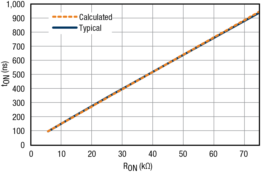
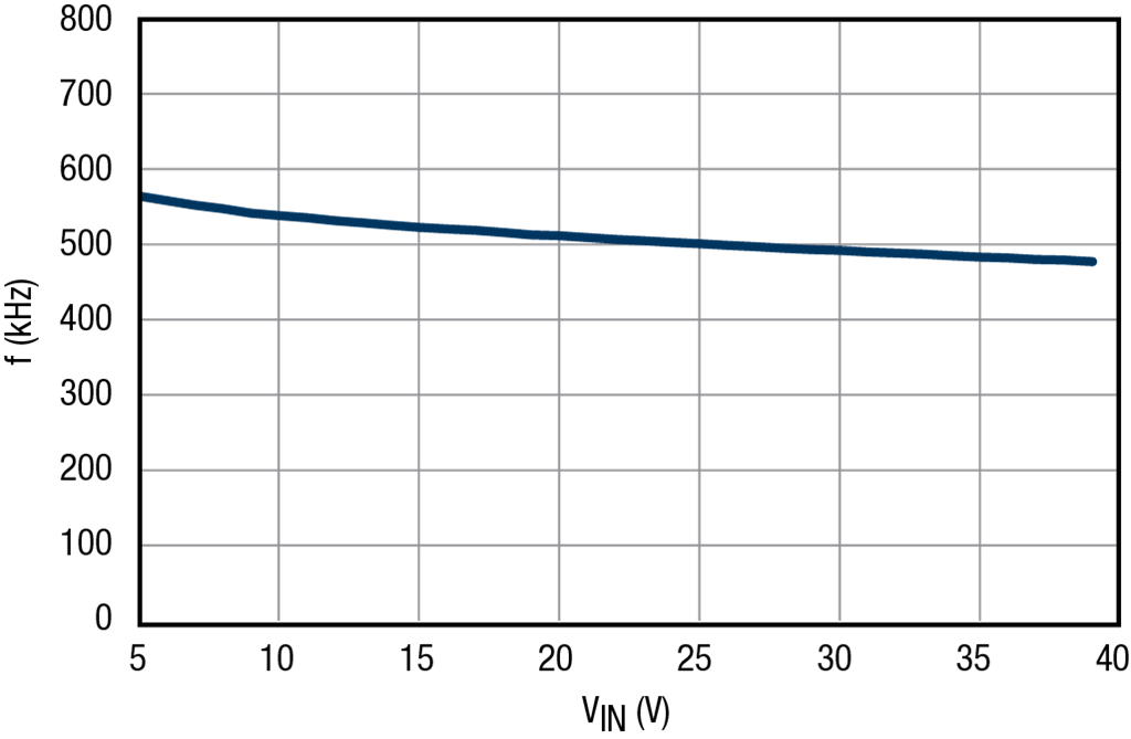
The correlation of this equation to the test data is also given in the datasheet. In the XR79206 example, Figure 5 in the Typical Performance Characteristics section shows very good correlation:


 In an ideal Buck Converter, tON is a function of VIN, VOUT and f expressed in following equation:


However, as no Buck Converter is ideal, test data is taken to determine a more accurate equation which is also given in the datasheet. In the XR79206 example, the following equation is given based on test data:


Substituting this tON equation into the above equation relating RON and tON and simplifying, we get:


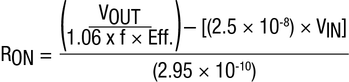
Then RON can be easily chosen based on the targeted VIN, VOUT, frequency and efficiency. So for example in the XR79206, if VIN = 24V, VOUT = 5V, f = 500kHz and efficiency = 90%,


The next closest commercially available resistor value can be used. Several RON examples are given in the datasheets based on the above equation for your convenience. For a given RON it should be noted that tON is inversely proportional to VIN. This inverse relationship allows the frequency to remain constant as VIN changes, except for some changes due to the non-ideal nature of the power components. For example, this is illustrated in the following graph from the XR79206:


As IOUT increases, frequency increases slightly due to increasing power losses. As losses increase, more power must be delivered per cycle to keep VOUT constant. Because tON is constant, the period decreases and frequency increases, as can be seen in the following example from the XR79206 datasheet:


Yes, the center pad should be connected to ground with a minimum of 5 vias to the GND plane (one at each corner and one in the middle). It is common to use 9 vias to GND (3 rows of 3 vias inside the pad). This helps thermal dissipation / conduction and electrical requirements for the device.

No, the maximum fault tolerance of the above devices is ±18V only. However, the XR3305x and XR3315x families DO support up to ±60V fault tolerance. To find the device in the XR3305x and XR3315x families with the configuration you are looking for, use the parametric search https://www.exar.com/products/interface/serial-transceivers/rs485-422. The Fault Tolerance column is on the right side of the table. See the filters on the left for device selection. See Application Note ANI-23 https://www.exar.com/ani-23.pdf for more on fault testing of these devices.

For any voltage above ±60V, refer to diode manufacturers, such as the Bourns RS-485 transient protection for example below, for an external diode to absorb the transient or surge voltage for protection.

https://www.digikey.com/product-detail/en/bourns-inc/RS-485EVALBOARD1/RS-485EVALBOARD1-ND/2658335

or

https://www.digikey.com/product-detail/en/bourns-inc/RS-485EVALBOARD2/RS-485EVALBOARD2-ND/2658336

Visit the product page for the part you are interested in.  The part's status is listed in the Parts & Purchasing section.  You can also view Product Lifecycle and Obsolescence Information including PDNs (Product Discontinuation Notifications).
 
To visit a product page, type the part into the search window on the top of the MaxLinear website.
 
In this example, we searched for XRA1201.  Visit the product page by clicking the part number or visit the orderable parts list by clicking "Orderable Parts". 


The Parts & Purchasing section of the product page shows the Status of all orderable part numbers for that product.  Click Show obsolete parts, to see all EOL or OBS products.


The XR17V35x device driver is dependent on the Generic multi-function driver being built into the Windows Embedded image. This driver is included by default in the desktop version of Windows, but not in the embedded versions.

The instructions for adding the Multi-function Driver are described by Microsoft:
https://msdn.microsoft.com/en-US/library/ff794057(v=winembedded.60).aspx

When using the native CDC-ACM driver the USB UARTs defaults to HW RTS/CTS flow control. Please see the datasheet:
https://www.exar.com/product/interface/uarts/usb-uarts/xr21b1422
section on CDC-ACM driver and Table 2.

You can test to see if there is data by grounding the CTS input.

USB peripheral devices may operate in bus or self-powered modes. In bus powered mode, the peripheral device is powered by the USB host 5V VBUS power either directly, or for example through a voltage regulator that might provide a regulated 3.3V to the device from the 5V VBUS input. In self-powered mode, power to the peripheral device comes from another source other than the USB host VBUS. For example, power might come from an AC to DC converter.


MaxLinear USB to serial / UART(s), USB hubs and USB to Ethernet devices all comply fully to USB standards and are fully USB compliance tested. One USB compliance test ensures that self-powered peripheral devices do not have “back voltage” when disconnected from the USB host, on either the USB data signals (USBD+ / USBD-) or the VBUS power itself.


All MaxLinear USB UARTs, hubs and USB to Ethernet devices are USB full speed or high-speed devices. As such, they have an internal pull-up on the USBD+ signal to “advertise” their speed rating. The VBUS_SENSE pin on these devices must be connected to VBUS from the host, or upstream device if that is not the host, such that the device “senses” the disconnection from the host or upstream device. The default power mode advertised to the USB host for all USB UARTs and USB to Ethernet devices is bus powered mode. Self-powered mode can be programmed in either the internal OTP memory or external EEPROM for self-powered mode. For MaxLinear hubs, an external pin controls the power mode advertised to the USB host, except the XR22417 which must always be operated in self-powered USB mode.

Connect the USB data pins directly to the host or upstream hub. Connections should be impedance controlled to 90 ohms differential with short traces and no stubs. Connecting any other components that are not high impedance (series or shunt resistance, capacitance or inductance) will corrupt the USB data signaling and can prevent communication between the host and device. ESD protection diodes may be used and some EMI filters may also have only a slight impact on impedance but should be demonstrated for compliance with USB 2.0 devices. See Application Notes AN202 (USB UART Board Design Recommendations and Considerations for USB Compliance), section 2.0 Design Considerations  for more. 

1. Native drivers: Native drivers may be found in all major OS such as Windows, Linux, and Max OSX. Typically these drivers will be automatically loaded. In some cases, these are basic drivers and may have limitations on advanced device functionality, however. USB HID, Hub and CDC-ACM drivers are examples of native drivers. The CDC-ACM driver be used with our CDC-ACM class USB UARTs, but has limited functionality.


2. MaxLinear custom drivers: MaxLinear custom drivers may be used to support additional functionality in MaxLinear devices. For example, the MaxLinear custom driver for USB UARTs overcomes the limitations of the native CDC-ACM driver. See https://www.exar.com/design-tools/software-drivers for a list of and access to the drivers that we currently have. In some cases, the MaxLinear driver can also be customized, or source code can be provided after executing a Software License Agreement.

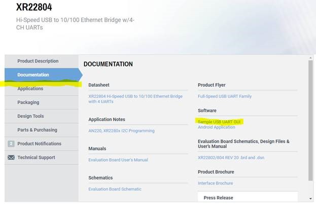
Yes: Go to the product page (XR22804 example below), click on the documentation tab on left, click on “Sample USB UART GUI” under Software:

 
Both Linux and Mac OSX have a native CDC-ECM driver which is automatically loaded and used by the XR2280x Ethernet function. Because Windows does not have a native CDC-ECM driver, MaxLinear supplies a custom driver, which can be found at https://www.exar.com/design-tools/software-drivers
It depends on the baud rate. For example, for a start bit, 8 data bits, no stop bit and 1 stop bit, the maximum baud rate deviation is 4.76%. For more information, see https://www.exar.com/appnote/dan108.pdf
The SP334 does not allow for both RS-232 and RS-485 protocols at the same time. Yes, it is correct in that if a termination resistor is used for RS-485 mode it must be fully removed from circuit during RS-232 mode. This can be done by using either relay or low resistance FET to connect / disconnect the termination resistor. The SP334 RS-485 protocol can be used for Half-duplex operation by connecting RXIN to TXout. If you wish to switch from Half-duplex to Full-duplex you will need a switch / relay for this operation or manual jumpers.
If the bypass pin is to be used, a 10nF ceramic capacitor is suggested. You may also use the value / type mentioned. The only concern with the bypass feature is that startup time is increased. If startup time is a concern then the bypass pin should be kept open. Different values of bypass capacitors will result in different startup times.
This is a little difficult to answer without knowing how the LED will be modulated. If the enable input is used for modulation it is possible that the device may not react fast enough to provide an output. This is very true if the Bypass pin is used. If the output load exceeds the current limit trip point, then the output will be turned off to protect the device. However if the output is always on and modulation is done with some external circuitry, then adding extra capacitance to the output could satisfy the current demand of the LED so as not to cause current limit activation.
Most UARTs use RTS#, however in addition to using the RTS# output as the Auto RS485 control output, the XR17C158, XR17D152/154/158 and XR17V258 can use the DTR# output as the Auto RS485 control output.
Most UARTs use RTS#, however in addition to using the RTS# output as the Auto RS485 control output, the XR17V352/354/358 can use the DTR# output as the Auto RS485 control output.
Most UARTs use RTS#, however in addition to using the RTS# output as the Auto RS485 control output, the XR21B1420/1421/1422/1424 can use the DTR# output as the Auto RS485 control output.
The EEPROM needs to have the PCI Vendor ID and Device ID, Subvendor ID and Subsystem Device ID. For more details, see DAN112 https://www.exar.com/appnote/dan112v100.pdf.

The SP485E offers enhanced ESD protection on RS-485 I/O lines (Driver output / Receiver input) up to ±15KV. The SP485 part does not offer this enhanced ESD protection level. All other electrical parameters are the same between each part.


The following lines of code must be modified in the xr_usb_serial_hal.c file in the xr_usb_serial_set_flow_mode function at the end of the function:


Change from:

xr_usb_serial_set_reg(xr_usb_serial, xr_usb_serial->reg_map.uart_flow_addr, flow);

xr_usb_serial_set_reg(xr_usb_serial, xr_usb_serial->reg_map.uart_gpio_mode_addr, gpio_mode);

 
For active low TX, change to:

xr_usb_serial_set_reg(xr_usb_serial, xr_usb_serial->reg_map.uart_flow_addr, 0x0);

xr_usb_serial_set_reg(xr_usb_serial, xr_usb_serial->reg_map.uart_gpio_mode_addr, 0x3);


For active high TX, change to:

xr_usb_serial_set_reg(xr_usb_serial, xr_usb_serial->reg_map.uart_flow_addr, 0x0);

xr_usb_serial_set_reg(xr_usb_serial, xr_usb_serial->reg_map.uart_gpio_mode_addr, 0xB);

All of MaxLinear / Exar's USB UARTs are CDC class / CDC-ACM compliant, except for XR21B1421 which is an HID class device. This means they can use a native CDC driver. All major OS have native CDC drivers, except Windows prior to Windows 10.

None of the MaxLinear / Exar USB UARTs require their custom driver, however they will have certain limitations when not using it. The native CDC driver is not capable of accessing the internal memory map of any device. As a result, when using the native CDC driver, the device “defaults” to a particular configuration. The main implications of this default configuration are that hardware RTS/CTS flow control is enabled and that other settings / advance settings are not configurable. Some devices, for example the XR21B1411 which has an internal OTP memory, can be programmed to change this default configuration, but the configuration cannot be changed “on the fly”.

The SP485E should behave in the same way as the SP485 part in any application. The Receivers offer a failsafe feature that when the inputs are floating the receiver output will be a logic high. If a termination resistor is used with this part, then a biasing network is needed to maintain the failsafe feature. The biasing network is the pull-up and pull-down resistors at RX input. When properly used, the biasing network will provide a differential voltage of greater than 200mV at Receiver input when the data cable is disconnected thus resulting in a logic high output. If this input has noise that is not common or if the input voltage to Receiver is between +/-200mV then its output will not respond correctly and can oscillate. Please ensure that during this problem the receiver input is greater than 200mV for correct output state.
1.  Enter root privileges: sudo -i
2.  Enter admin password.
3.  Edit /etc/modules file.  Append xr_usb_serial_common to the end of the file.
4.  Build the Exar/MxL driver from the folder using "make", confirm that the xr_usb_serial_common.ko file is successfully created.
5.  Run command: uname -r
This will return the kernal version currently in use. 
6.  Copy the resulting xr_usb_serial_common.ko to /lib/modules/2.6.38.8-generic in the above path with the kernal version that was returned in step 5.
7.  Run depmod.
8.  Reboot. 
9.  Connect the Exar/MxL USB UART.  Using ls/dev/tty* confirm /dev/ttyUSBn ports (Exar driver loaded) for Exar/MxL USB UART.
10. Connect another CDC device (not Exar/MxL), and confirm both /dev/ttyUSBn and /dev/ACMn ports. 
The maximum allowed bus-powered suspend current is 2.5mA per device function. The device function may not be the same as the IC, as there may be multiple device functions per IC. See the individual datasheet for a list of device functions. For example, the XR22804 has 8 device functions: an embedded hub, the Ethernet MAC and Phy, 4 UARTs, I2C controller and EDGE controller. Therefore, the XR22804 maximum allowed bus-powered suspend current is 8 x 2.5mA or 20mA. However, power used by all supporting XR22804 external components that use power from the USB host VBUS power must be included in the suspend current.
The external EEPROM can be used to modify various USB configuration descriptors such as the Vendor ID, Product ID, Device Attributes and maximum power consumption. See Application Note AN202 (USB UART Board Design Recommendations and Considerations for USB Compliance), section 2.3 External EEPROM or on-chip OTP for more.
The OTP can be programmed to modify various USB configuration descriptors such as Vendor ID, Product ID, Device Attributes and maximum power consumption. See Application Note AN202 (USB UART board Design Considerations for USB Compliance), section 2.3 External EEPROM or on-chip OTP for more. The OTP can also be programmed to change default register values, which can be found in the individual datasheets.

The COT families (XRP6141, XRP6124 and XR75100 controllers, XR76xxx regulators and XR79xxx power modules) have 2 modes of operation that can be set: DCM / CCM (discontinuous conduction mode / continuous conduction mode) or FCCM (Forced CCM) mode. In FCCM mode, the converter operates at a preset frequency regardless of output current. In DCM / CCM mode the converter operates in DCM or CCM depending on the Iout magnitude. If Iout < ½ Ipp, the converter transitions to DCM mode. If Iout is higher, operation is in CCM mode.

The main advantage of DCM / CCM is that it provides significantly higher efficiency at light loads. For those applications where that doesn’t matter, FCCM can be used and has the advantage that it allows for operation at a constant frequency, regardless of load. It also results in lower Vout ripple, and will operate in an inaudible range.

Use the VSNS pin to monitor VOUT as described in the Overvoltage Protection section of the datasheet., which is on page 13:
 

Size the inductor for 30% to 40% peak-to-peak inductor current ripple.

Size Cout for required load step transient response, for example <3% VOUT transient for a 0 – 50% rated current. Cout also needs to be sized for steady state output voltage ripple. Use effective value of capacitors corresponding to operating conditions.

Place small signal components close to their respective pins.

Place CIN capacitors close to PVIN / PGND pins.

Place inductor close to SW pin in order to reduce switching noise from this pin. Also keep the SW pin landing pad area as small as possible.

Size Cout for required load step transient response, for example <3% VOUT transient for a 0 – 50% rated current. Cout also needs to be sized for steady state output voltage ripple. Use effective value of capacitors corresponding to operating conditions.

Place small signal components close to their respective pins.

Place CIN capacitors close to PVIN / PGND pins.

There are many factors to consider in selecting the inductor including core material, inductance versus frequency, current handling capability, efficiency, size and EMI. Typically, the inductor is primarily chosen for value, saturation current and DC resistance (DCR). Increasing the inductor value will decrease output voltage ripple, but degrade transient response. Low inductor values provide the smallest size, but cause large ripple currents, poor efficiency and require more output capacitance to smooth out the larger ripple current. The inductor must be able to handle the peak current at the switching frequency without saturating, and the copper resistance in the winding should be kept as low as possible to minimize resistive power loss. A good compromise between size, loss and cost is to set the inductor ripple current to be within 20% to 40% of the maximum output current.


The switching frequency and the inductor operating point determine the inductor value as follows:


L = Vout x (Vinmax – Vout) / Vinmax x fs x Kr x Ioutmax


Where fs = switching frequency

Kr = ratio of the AC inductor ripple current to the maximum output current


So for example, we want to choose L for the XR76108 (Ioutmax 8A) and wish to convert 12Vin to 2.5Vout with a frequency of 1MHz:


L = 2.5V x (12V – 2.5V) / 12V x 106 x 35% x 8A = 0.707 uH


The peak-to-peak inductor ripple current is:


Ipp = Kr x Ioutmax
 

In our example, Ipp = 35% x 8A = 2.8A


Once the required inductor value is selected, the proper selection of core material is based on peak inductor current and efficiency requirements. The core must be large enough not to saturate at the peak inductor current.


Ipeak = Ioutmax + Ipp/2

In our example, Ipeak = 8A + 2.8A/2 = 9.4A

 
and provide lower core loss at the high switching frequency. Low cost powered-iron cores have a gradual saturation characteristic but can introduce considerable AC core loss, especially when the inductor value is relatively low and the ripple current is high. Ferrite materials, although more expensive, have an abrupt saturation characteristic with the inductance dropping sharply when the peak design current is exceeded. Nevertheless, they are preferred at high switching frequencies because they present very low core loss while the designer is only required to prevent saturation. In general, ferrite or molypermalloy materials are a better choice for all but the most cost sensitive applications.
See Application Note ANP-20 (Properly Sizing MOSFETs for PWM Controllers).

In general, it is set for Imax x 1.5. It would be close the maximum Iout (including ripple). If conservatively set too high, the hiccup mode may not be activated fast enough. If set too low, the ripple could cause the current to go over the threshold and set it into hiccup on a pre-mature basis.


The datasheets have an equation that calculates the Rlim resistor value to be used to program the Iocp. Also, a graph of Iocp vs. I lim is shown in the datasheet.

A zero-cross comparator monitors the voltage across the low-side FET when it is on. The comparator threshold is nominally set at -1mV or -2mV (see individual datasheet). If there is sufficient IOUT such that VSW is below the threshold and therefore does not trigger the zero-cross comparator, CCM operation continues.


As IOUT is reduced, VSW gets closer to ground. When VSW meets the threshold, the zero-cross comparator triggers. If there are 8 consecutive triggers, then DCM operation begins. The low side FET is turned off when IL x RDS equals the zero-cross threshold.


As there is no negative inductor current, the charge transferred to COUT is preserved. As IOUT decreases further, less charge transfer to COUT is required. Pulses grow further apart, frequency is reduced and efficiency increases.


DCM persists as long as there are 8 consecutive zero-crosses.


Note that when the DCM frequency falls below about 1kHz, the controller turns on the lower-side FET for 100ns once every 1.2ms to refresh the charge on the bootstrap capacitor. This refresh cycle generates small spikes on SW, which can be seen interlaced between DCM pulses.

For best gate drive performance, it is recommended to route GL_RTN (PGND) together with its GL pin like a differential pair instead of just connecting GL_RTN to GND at the IC and subjecting it to ground noise. Routing them together cancels out any noise, inductive and electromagnetic field effects between these two traces. See ANP-32 Practical Layout Guidelines for PowerXR Designs http://www.exar.com/appnote/anp32 page 8 for more information.

For thermal and ESD benefits, the following PCB design is recommended to provide thermal and electrostatic paths:


1. Design the PCB to conduct heat away from the device using thermal vias under the QFN IC to the digital ground plane.

2. Mount the metal shells of the USB and Ethernet connectors to a separate Chassis / Earth ground.

3. Place the chassis / earth ground metal on one PCB layer, digital ground on another PCB layer and connect through a zero ohm resistor located away from sensitive electronic devices as much as possible.

4. Place a large metal trace for the Earth ground all the way surrounding the PCB, except under the Ethernet connector.


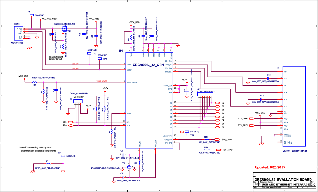
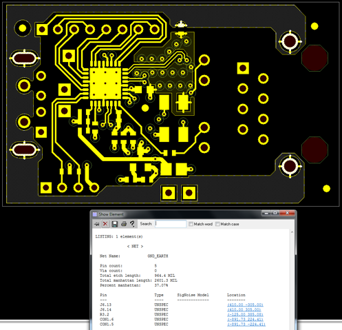
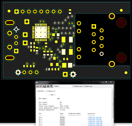
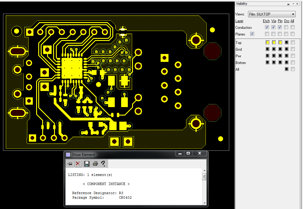
As an example, see the schematic and an example PCB layout for the XR22800 Evaluation Board below:

 
Schematic: 
  
 
Layer 1 Chassis / Earth ground layout with mounting pins for Ethernet and USB metal shells: 


Layer 2 Digital ground layout:


Stackup layout with zero ohm resistor connecting Earth and Digital ground: 


Please check that all the following conditions are satisfied first.


  • no interrupts pending (ISR bit-0 = 1)
  • modem inputs are not toggling (MSR bits 0-3 = 0)
  • RX input pin is idling HIGH • divisor (the value in DLL register) is non-zero
  • TX and RX FIFOs are empty


Be sure sleep mode bit has been set to 1. If there are multiple UART channels, the sleep conditions must be true for all channels.


See more on Sleep Mode in AN204 UART Sleep Mode.

Yes. Note: some devices do have powersave mode. If UART goes into powersave mode, then the registers are not accessible.


See more on Sleep Mode in AN204 UART Sleep Mode.

Read LSR register to check whether the UART receives the data or not.


  • If LSR value is 0x60, it means that either UART receiver FIFO doesn’t receive the data or the data in receiver FIFO has been read out before the read of LSR.
  • If LSR value is 0x00, it means data is still in the THR (clock doesn’t oscillate to transmit data).
  • If LSR value is 0xFF, it means either UART is in powersave mode or UART is powered off. For those devices with powersave mode, be sure that UARTS are not in powersave mode.


See more on Sleep Mode in AN204 UART Sleep Mode.


  • Check whether the register set can be accessed.
  • Check whether the crystal is oscillating fully.
  • Check whether the data can be transmitted in internal loopback mode.


See more on Sleep Mode in AN204 UART Sleep Mode.

Once enumeration is completed, the host and device may carry out data transfers. Four type of data transfers are defined: control, bulk data transfers, interrupts and Isochronous data transfers. Although USB UARTs do support the control, bulk data transfers and interrupts, they do not support Isochronous data transfers which would be needed for applications streaming audio or video. See Application Note AN213 (section 3.3.2) for a description of each.
Although the MPIO driver and the first COM port of the PCIe UART share the same memory allocation, the resource conflict is not an issue because the MPIO driver and the COM port driver do not access any of the same register addresses. Note that, with this "memory conflict" warning message, the driver has passed Windows WHQL certification testing.